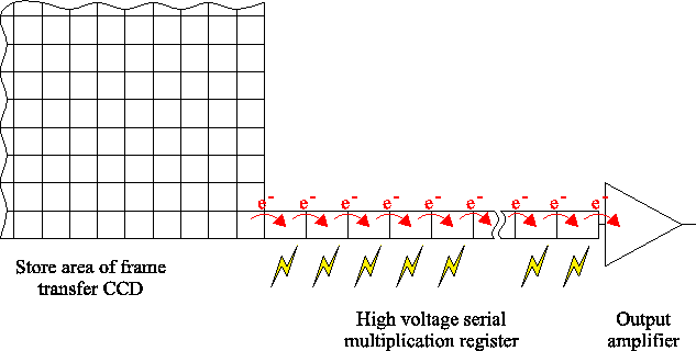
L3Vision CCDs have a relatively standard frame-transfer CCD structure
but have an output register which has been extended with an additional
section called the ``multiplication register'', as shown in
Figure 4.1. In the multiplication register one of the
three phases is clocked with a much higher voltage than is needed
purely for charge transfer (typically  --
--
 ). The large
electric fields which are established within the semiconductor
material accelerate charge-carrier electrons to sufficiently high
velocities that additional carriers can be generated by impact
ionisation, as described in Jerram et al. (2001); Burt & Bell (1998). This generates a
small level of charge multiplication (signal gain) in each stage of
the high-voltage multiplication register. The large number of gain
stages in the register can lead to a substantial overall gain in
signal level. The output of the multiplication register is read out
using a conventional CCD amplifier. Measurements in the laboratory did
not show any signs of non-linearity in the multiplication register
when the CCDs were operated at signal levels well below saturation
(Mackay et al. , 2001).
). The large
electric fields which are established within the semiconductor
material accelerate charge-carrier electrons to sufficiently high
velocities that additional carriers can be generated by impact
ionisation, as described in Jerram et al. (2001); Burt & Bell (1998). This generates a
small level of charge multiplication (signal gain) in each stage of
the high-voltage multiplication register. The large number of gain
stages in the register can lead to a substantial overall gain in
signal level. The output of the multiplication register is read out
using a conventional CCD amplifier. Measurements in the laboratory did
not show any signs of non-linearity in the multiplication register
when the CCDs were operated at signal levels well below saturation
(Mackay et al. , 2001).
Figure 4.1:
Electrons are transferred serially through the gain stages making up
the multiplication register of an L3Vision CCD. The high voltages
used in these serial transfers induce the creation of additional charge
carriers through impact ionisation.
 |
Bob Tubbs
2003-11-14